Femto Laser Cutting
Femto Laser Cutting
Got it, here’s the translation and paraphrasing:
- 1 millisecond (ms) = 0.001 seconds = 10^-3 seconds
- 1 microsecond (μs) = 0.000001 seconds = 10^-6 seconds
- 1 nanosecond (ns) = 0.000000001 seconds = 10^-9 seconds
- 1 picosecond (ps) = 0.000000000001 seconds = 10^-12 seconds
- 1 femtosecond (fs) = 0.000000000000001 seconds = 10^-15 seconds
Understanding these units of time, we know that femtosecond lasers are a type of extremely short-pulsed laser cutting. In the past decade, the technology of ultra-short pulse femtosecond laser cutting has made significant progress.
Significance of Ultra-Short Pulse Lasers
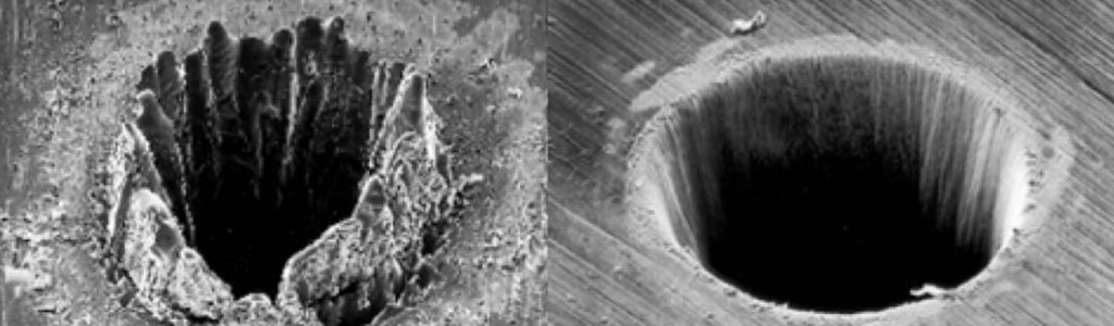
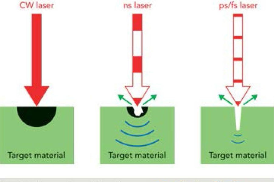
People have long attempted to use lasers for micro-processing. However, the long pulse width and low laser intensity of traditional lasers result in material melting and continuous evaporation. Although the laser beam can be focused into a small spot, the significant thermal impact on the material limits processing accuracy. Only by reducing thermal effects can processing quality be improved.
When lasers with pulse durations on the order of picoseconds interact with materials, significant changes in processing occur.
As the pulse energy rises sharply, the high power density is sufficient to strip outer electrons. Since the interaction time between the laser and the material is very short, ions are ablated from the material surface before transferring energy to the surrounding material, thus avoiding thermal impacts and also known as “cold processing.” With the advantages brought by cold processing, short and ultra-short pulse lasers have entered industrial production applications.
Ultra-short pulse processing rapidly injects energy into a very small area of action. The instantaneous high energy density deposition changes the way electrons absorb and move, avoiding effects such as laser linear absorption, energy transfer, and diffusion, fundamentally changing the interaction mechanism between the laser and the material.
Wide Applications of Laser Cutting
Wide Applications of Laser Cutting
Laser processing includes high-power cutting, welding; micro-processing such as drilling, scribing, cutting, texturing, stripping, isolation, etc. The main uses of various laser processing methods include:
Drilling
In circuit board design, ceramic substrates are used instead of conventional plastic substrates to achieve better thermal conductivity. To connect electronic components, it’s generally necessary to drill hundreds of micrometer-level holes on the board. Therefore, ensuring the stability of the substrate during drilling is crucial, and picosecond lasers are ideal tools for this application.
Picosecond lasers can drill holes through a process of percussion drilling while ensuring the uniformity of the holes. In addition to circuit boards, picosecond lasers can also be used for high-quality drilling of materials such as plastic films, semiconductors, metal films, and sapphire.
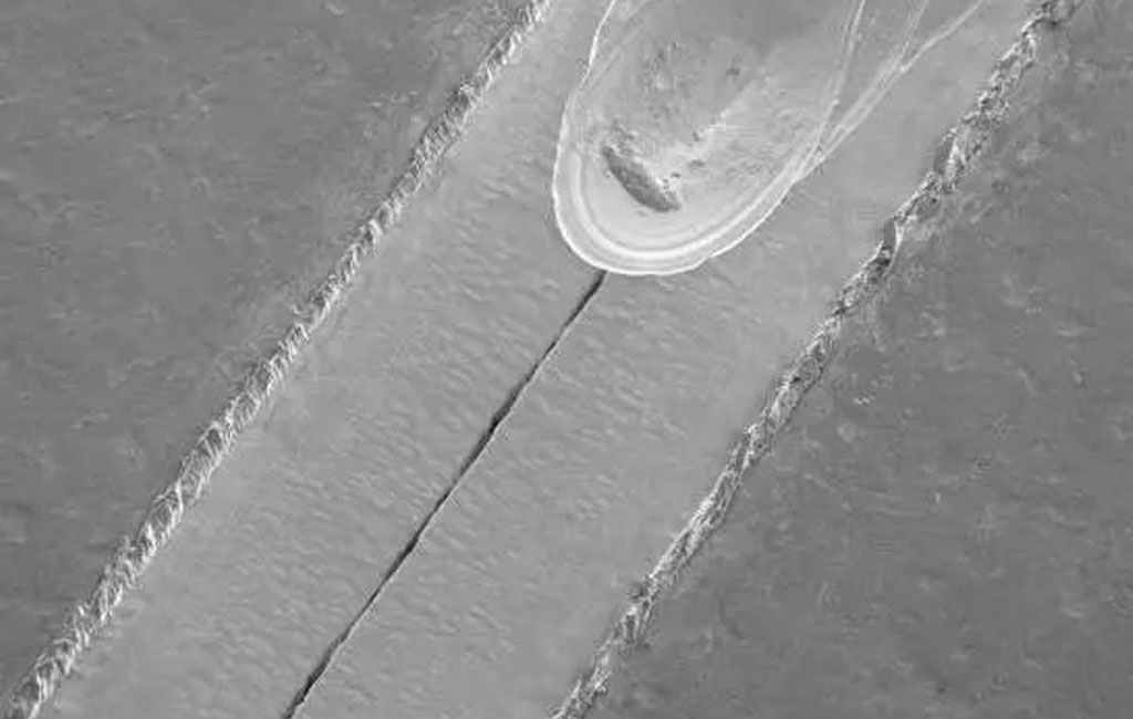
Scribing, Cutting
Lines can be formed by overlaying laser pulses through scanning. Usually, a large number of scans can penetrate into the interior of ceramics until the depth of the lines reaches 1/6 of the material thickness. Then individual modules are separated from the ceramic substrate along these scribe lines. This separation method is called scribing.
Another separation method is using ultra-short pulse laser ablation cutting, also known as melt cutting. The laser ablates the material until it is cut through. The advantage of this technique is that the shape and size of the processed holes have greater flexibility. All process steps can be completed with a picosecond laser.
Different effects of picosecond and nanosecond lasers on line scribing in polycarbonate materials.
Line Ablation (Coating Removal)
Another application often considered micro-processing is to precisely remove coatings without damaging or slightly damaging the base material. Ablation can be either a few micrometers wide line or a large area removal of several square centimeters.
Since the thickness of the coating is usually much smaller than the width of the ablation, so that heat cannot be conducted laterally. Therefore, lasers with nanosecond pulse widths can be used.
The combination of high average power lasers, square or rectangular beam delivery fibers, and flat-top intensity distribution allows laser surface ablation to be applied in industrial fields. For example: using the TruMicro 7060 laser from Trumpf to remove coatings on thin-film solar cell glass. The same laser can also be applied in the automotive industry to remove corrosion coatings in preparation for subsequent welding.
Surface Structuring
Structuring can change the physical properties of material surfaces. According to the lotus effect, hydrophobic surface structures allow water to flow off the surface. Creating submicron structures on the surface with ultra-short pulse lasers can achieve this property and can precisely control the structures to be created by changing laser parameters.
Conversely, the opposite effect, such as hydrophilic surfaces, can also be achieved, and micro-processing can create larger structures. These processes can be used to manufacture microstructures in oil tanks in engines to reduce wear, or to structure metal surfaces for bonding with plastics.
Engraving Forming
Engraving forming creates three-dimensional shapes by ablating materials. Although the size of the ablation may exceed the traditional scope of micro-processing, the precision required categorizes it into this class of laser applications. Picosecond lasers can be used to process the edges of polycrystalline diamond tooling on milling machines.
Laser is an ideal tool for processing polycrystalline diamond, an extremely hard material used for milling cutters. Using engraving forming technology to process chip grooves and teeth on milling cutters, the advantage of laser in this case is non-contact and high processing accuracy.
Micro-processing has a very broad application prospect, and more and more consumer products are entering our field of vision through laser micro-processing.
Laser processing is a non-contact processing method with significant advantages such as fewer subsequent processes, good controllability, easy integration, high processing efficiency, low material loss, and low environmental pollution. It has been widely used in industries such as automotive, electronics, electrical appliances, aviation, metallurgy, and mechanical manufacturing, playing an increasingly important role in improving product quality, labor productivity, automation level, and reducing material consumption.
Our Femto Laser Cutting Partner and Laboratory
Our Partner and laboratory(Be-Cu prototype company)is fully equipped and ready to handle any femtosecond laser micromachining and stent laser cutting task. Whether it is a prototype to test your idea, small to medium-scale production services, or a need for a tailor-made laser system – we are ready to assist.
Be-Cu guarantee ultra-high precision and quality micron-range results on diverse materials – all types of glass, sapphire, silicon, ceramic, metal, polymer, optical fibers, diamond, etc.
A wide range of femtosecond laser micromachining applications perform in our lab: laser micro drilling, laser micro cutting, selective laser induced etching (SLE), laser welding, surface structuring, volume modifications, laser micro marking, MPP multiphoton polymerization, etc.
Be-Cu’s Femtosecond Laser is the go-to choice for precision micro feature machining, often deployed to infuse intricate details into Swiss-turned or wire EDM micro components. Be-Cu has showcased its prowess in achieving hole diameters under 25 microns and slots under 20 microns. The majority of holes can maintain their cylindrical form up to 8-10 times their diameter. With capabilities boasting less than 1 micron accuracy and repeatability, this equipment is a game-changer.
Be-Cu, LLC employs femtosecond laser processing to cater to the needs of the medical, aerospace, energy, and microelectronics sectors. The stability and adaptability of the Femto laser have enabled Be-Cu to sculpt parts and materials with a finesse that traditional machining methods could only dream of. The Femtosecond Laser’s knack for handling a wide array of materials while consistently delivering spot-on results offers unparalleled flexibility in the design realm. Be-Cu’s team of process engineers revels in the challenge of exploring new materials with the Femto Laser, leveraging their expertise to push boundaries. The unmatched precision and accuracy of Be-Cu’s Femtosecond Laser position it as the ultimate solution for micro feature machining needs and applications.